If you've got an FPGA you synthesize HDL for, this is the thread for you.

Discuss all aspects of FPGA development, including tips, tricks, and questions for the experts among us.
I had an old Basys2 board with a Spartan3E on it, but the thing had grounding issues so I ended up having to get the new Basys3, which has an Artix7. There's significantly more block RAM on board, and the IDE they provide is a lot different from the one I was used to using back in high school.
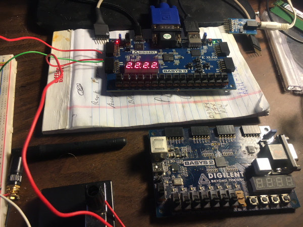
(click for full res. basys3 is above running the self test while the basys2 is below it)
It's been a difficult adjustment since I'd been using the Basys2 for so long and I'd been used to it, but overall the Basys3 has a lot of nice features if you're still a novice at this kind of stuff. A bit disappointing is that the USB HID is just a microcontroller interface that emulates PS/2 with the FPGA rather than just a passthrough that manages the base HID protocol, but I've got a raw USB type A female pinned out for a breadboard.
Short term projects I'd like to finish include an implementation of conway's game of life, a morse code interpreter (found an old key at a surplus store, been practicing), and some web interfaces as a proof of concept since I've got both a cheap chinky full TCP stack low power wifi passthrough chip as well as a real raw 10/100 ethernet that's only got the MAC layer, which I want to practice implementing the UDP/IP and TCP/IP layers on top of.
The end goal would hopefully be to create a custom processor architecture running on the FPGA that I'll write an assembler for on my main OS, then an operating system. It'll be quite a while before that happens and I doubt it'll be on the Basys3, but damn it would be bitchin.

Discuss all aspects of FPGA development, including tips, tricks, and questions for the experts among us.
I had an old Basys2 board with a Spartan3E on it, but the thing had grounding issues so I ended up having to get the new Basys3, which has an Artix7. There's significantly more block RAM on board, and the IDE they provide is a lot different from the one I was used to using back in high school.
(click for full res. basys3 is above running the self test while the basys2 is below it)
It's been a difficult adjustment since I'd been using the Basys2 for so long and I'd been used to it, but overall the Basys3 has a lot of nice features if you're still a novice at this kind of stuff. A bit disappointing is that the USB HID is just a microcontroller interface that emulates PS/2 with the FPGA rather than just a passthrough that manages the base HID protocol, but I've got a raw USB type A female pinned out for a breadboard.
Short term projects I'd like to finish include an implementation of conway's game of life, a morse code interpreter (found an old key at a surplus store, been practicing), and some web interfaces as a proof of concept since I've got both a cheap chinky full TCP stack low power wifi passthrough chip as well as a real raw 10/100 ethernet that's only got the MAC layer, which I want to practice implementing the UDP/IP and TCP/IP layers on top of.
The end goal would hopefully be to create a custom processor architecture running on the FPGA that I'll write an assembler for on my main OS, then an operating system. It'll be quite a while before that happens and I doubt it'll be on the Basys3, but damn it would be bitchin.
Figured I'd share a discovery I just made here for any other folks like me that are new to this kind of stuff, as you might run into the same thing. It's very hard to find resources for this online, and it took me a while to figure this one out.
When I was dividing the main clock signal on my Basys2, I'd usually just set up a module with a prescaler that'd flip the clock signal from positive to negative once it reached zero. Since the highest frequency item that I was dealing with was writing the VGA signal out at 25 MHz, this worked perfectly fine, though due to it using flip-flops on the system it was susceptible to skew due to propagation delays in the FETs.
However when I upgraded the IDE after I got the Basys3 I discovered that there's a large number of primitive module types that are synthesized directly to features on the FPGA that are far more optimized than anything that could be done through the programmatic configuration of the gates. One of the things I discovered were PLLs and MMCMs.
PLL is short for phase-locked loop; folks that have worked with signal processing are familiar with this one. Essentially, a PLL is a circuit that synchronizes the phases of multiple clock signals of varying frequencies. In any complex digital system this is essential, as you will be frequently passing around different clocks to different parts of your circuit in which the frequencies of the clocks vary, yet the rising edges of each need to fire in each component they're wired to at predictable cycles with respect to the master clock.
MMCM is short for mixed-mode clock manager and is a superset of the PLL, meaning that it is more generalized form of that construct. MMCMs function identically to clock trees in other digital signal systems, and are often used to distribute various clock nets across the circuit. You're given a few more options with the MMCM primitive, and for most circumstances this primitive is what you'll be using for generating all the frequencies you need in the clock tree for your circuit.
An interesting property of PLLs and by extension MMCMs is that they can generate higher frequency signals than what is supplied by the master clock signal. When I first read this, it didn't make much sense to me since I figured they were just simple divider circuits, but they aren't. Frankly I still don't fully understand how or why this is possible but for the sake of what I'll be discussing this is very relevant.
Consider the circumstance where you have a master clock of frequency 100 MHz. You need to generate a clock of frequency 25.175 MHz to drive a 640x480 VGA display at 60 Hz. Using an MMCM, you may be tempted to do this:
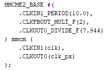
Here we're saying that for our MMCM named mmcm, we're supplying a clock with an input period of 10 nanoseconds (which is correct), we multiply the frequency of the input clock in the feedback portion of the phase-locked loop by 2, increasing it to 200 MHz. From that point, we'd like to divide our phase-locked clock by 7.944 (which is 200 MHz / 25.175 MHz) so that clk_px is supplied with a 25.175 MHz signal.
In theory, this makes sense. In practice, you will get this error on the implementation step:

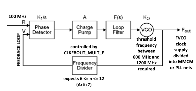
Why is this? As it turns out, the onboard MMCM systems on all FPGA chips have a specific frequency range that the voltage-controlled oscillator in any PLL or MMCM primitive must be within prior to dividing the voltage to obtain your required output. What this error is telling us is that the frequency that the voltage-controlled oscillator within the MMCM/PLL must lie between 600 MHz and 1200 MHz. This means, for the value of CLKFBOUT_MULT_F we must supply it with a value inclusively between 6.0 and 12.0. In turn, this means that we must adjust our division to CLKOUT0 so that it's based on this threshold of internal frequency on the voltage controlled oscillator.
Pictured is a block diagram of a phase-locked loop. This should illustrate roughly what's happening, note that this is only the component that generates the higher frequency intermediary, the signal would then be divided into each respect MMCM or PLL clock output.
Given this, a possible correct implementation of this would be as follows:
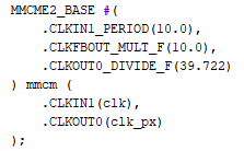
Here we're saying that for mmcm, we're supplying a clock with an input period of 10 nanoseconds (still correct), multiplying that frequency by 10 to satisfy the requirement of the FPGA for the voltage controlled oscillator, and then based on that we then divide this 1000 MHz signal by 39.722 to achieve our desired 25.175 MHz output signal on clk_px.
Hopefully this helped someone, I was stuck for a few hours trying different things until I finally figured this out on accident. If I find out more info about this, I will update this post.
When I was dividing the main clock signal on my Basys2, I'd usually just set up a module with a prescaler that'd flip the clock signal from positive to negative once it reached zero. Since the highest frequency item that I was dealing with was writing the VGA signal out at 25 MHz, this worked perfectly fine, though due to it using flip-flops on the system it was susceptible to skew due to propagation delays in the FETs.
However when I upgraded the IDE after I got the Basys3 I discovered that there's a large number of primitive module types that are synthesized directly to features on the FPGA that are far more optimized than anything that could be done through the programmatic configuration of the gates. One of the things I discovered were PLLs and MMCMs.
PLL is short for phase-locked loop; folks that have worked with signal processing are familiar with this one. Essentially, a PLL is a circuit that synchronizes the phases of multiple clock signals of varying frequencies. In any complex digital system this is essential, as you will be frequently passing around different clocks to different parts of your circuit in which the frequencies of the clocks vary, yet the rising edges of each need to fire in each component they're wired to at predictable cycles with respect to the master clock.
MMCM is short for mixed-mode clock manager and is a superset of the PLL, meaning that it is more generalized form of that construct. MMCMs function identically to clock trees in other digital signal systems, and are often used to distribute various clock nets across the circuit. You're given a few more options with the MMCM primitive, and for most circumstances this primitive is what you'll be using for generating all the frequencies you need in the clock tree for your circuit.
An interesting property of PLLs and by extension MMCMs is that they can generate higher frequency signals than what is supplied by the master clock signal. When I first read this, it didn't make much sense to me since I figured they were just simple divider circuits, but they aren't. Frankly I still don't fully understand how or why this is possible but for the sake of what I'll be discussing this is very relevant.
Consider the circumstance where you have a master clock of frequency 100 MHz. You need to generate a clock of frequency 25.175 MHz to drive a 640x480 VGA display at 60 Hz. Using an MMCM, you may be tempted to do this:
Here we're saying that for our MMCM named mmcm, we're supplying a clock with an input period of 10 nanoseconds (which is correct), we multiply the frequency of the input clock in the feedback portion of the phase-locked loop by 2, increasing it to 200 MHz. From that point, we'd like to divide our phase-locked clock by 7.944 (which is 200 MHz / 25.175 MHz) so that clk_px is supplied with a 25.175 MHz signal.
In theory, this makes sense. In practice, you will get this error on the implementation step:
Why is this? As it turns out, the onboard MMCM systems on all FPGA chips have a specific frequency range that the voltage-controlled oscillator in any PLL or MMCM primitive must be within prior to dividing the voltage to obtain your required output. What this error is telling us is that the frequency that the voltage-controlled oscillator within the MMCM/PLL must lie between 600 MHz and 1200 MHz. This means, for the value of CLKFBOUT_MULT_F we must supply it with a value inclusively between 6.0 and 12.0. In turn, this means that we must adjust our division to CLKOUT0 so that it's based on this threshold of internal frequency on the voltage controlled oscillator.
Pictured is a block diagram of a phase-locked loop. This should illustrate roughly what's happening, note that this is only the component that generates the higher frequency intermediary, the signal would then be divided into each respect MMCM or PLL clock output.
Given this, a possible correct implementation of this would be as follows:
Here we're saying that for mmcm, we're supplying a clock with an input period of 10 nanoseconds (still correct), multiplying that frequency by 10 to satisfy the requirement of the FPGA for the voltage controlled oscillator, and then based on that we then divide this 1000 MHz signal by 39.722 to achieve our desired 25.175 MHz output signal on clk_px.
Hopefully this helped someone, I was stuck for a few hours trying different things until I finally figured this out on accident. If I find out more info about this, I will update this post.
Recently I started a HDL class at uni, so I finally got access to an fpga to work on. We were supposed to do a project, but thankfully the list we were supposed to pick from had an option to suggest your own. I opted for a simple synthesizer, with a few volume-controlled square channels and a noise channel. Less capable than a Famicom! (it's OK, the other projects were stuff like "kitchen timer")
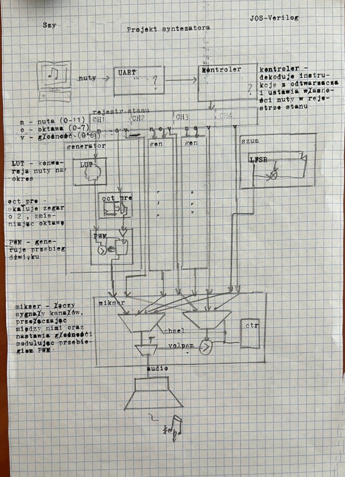
Here is a block diagram I submitted first – typewritten because quirky. The generator channels create 1-bit waveforms (square or noise), which is then mixed by switching between them and volume controlled via another layer of PWM. I also intend to route the per-channel volume signals to blinkenlights. The entire thing is controller by a register bank, which a controller will write to, ideally based on UART signals from a player on a computer.
Today I finally managed to get some sound out of it, with the generators and mixer working. I don't have the controller part yet, and my UART is untested. I instead converted an XM i wrote to a stream of state register values and put it in ROM.
It's all an octave too high and the noise channel basically can't be heard, but it's a neat PoC.
On Friday I finished it and submitted it for the class. You can see the source code at my Gitea. There's a keyboard and player demo.
I also arranged four songs for the player, but you don't get to know about two of them. Here's a video of it playing Jožin z bažin, a Czechoslovak song that was a meme in Poland a decade and a half ago and was randomly on my mind the night before.
In the previous video (and all pre-UART tests of the player) I used Cirno's theme to test. Here's a video of it being beamed to the chip via UART as always inteded. Sadly, due to framing you can't see the blinkenlights.
Here's one more video, of the keyboard thing. It directly tries to play key events (mapped to piano keys, as shown on the cheatsheet on-screen!) with a simple envelope. The numpad numbers are mapped to the noise channel instead, you can hear it can also be (somewhat) pitched. Annoyingly, I did not get the actual keyboard in frame.
Sorry about the quality of these. I don't have a FPGA at home (which is, by the way, the main reason I was excited for this project), so all had to be done in class. I also used university computers, because Vivado weighs a hundred gigabytes now, and I do not want that on my computer. For local development and smaller tests (via testbenches) I used Icarus Verilog, and to check if the stuff I wrote could even be synthesized I tried modules in DigitalJS.
Altogether, had fun.
This is cool, I really want to mess with FPGAs myself sometime
The instructions are the last resort.
very well done on this project, the code is very clean as well. it's really cool that you picked up on fpga dev because it was the last electronics related thing i truly enjoyed studying before my indefinite hiatus in the field so i absolutely love seeing writeups like this. i hope you will do moar in the future
more FPGA project shenanigans at uni, an analog VGA clock
found myself needing another project, i wanted to make something graphical this time (and also was sick on beating on the synth topic) and came up with an analog clock. the interesting parts were the VGA signaling (trivial) and CORDIC to turn angles into pixel positions. i didnt have a good idea for the line rendering, so i just draw a couple of squares along the pointer. the background is a variation on the old XOR trick, but with time added in -
i ended up really speedrunning this one, i decided on and confirmed the topic last wednesday, did some initial implementations and simulations at home, and today i first got to a real FPGA and managed to hand the implementation in after 7h of stinking up the classroom. i was really happy when both the VGA timing and CORDIC worked immediately lol. all in all just under a week - one of the few times at uni i'm early with something. or not quite yet, i still have to write a report...
found myself needing another project, i wanted to make something graphical this time (and also was sick on beating on the synth topic) and came up with an analog clock. the interesting parts were the VGA signaling (trivial) and CORDIC to turn angles into pixel positions. i didnt have a good idea for the line rendering, so i just draw a couple of squares along the pointer. the background is a variation on the old XOR trick, but with time added in -
(((x+t)^y)+t)&0xFi ended up really speedrunning this one, i decided on and confirmed the topic last wednesday, did some initial implementations and simulations at home, and today i first got to a real FPGA and managed to hand the implementation in after 7h of stinking up the classroom. i was really happy when both the VGA timing and CORDIC worked immediately lol. all in all just under a week - one of the few times at uni i'm early with something. or not quite yet, i still have to write a report...